
AZO Nanoparticles Sintering
Aluminum-doped zinc oxide has been chosen for this research due to its high conductivity, availability, low cost, and minimal environmental impact. It has emerged as a promising thermoelectric material. In this study, a laser with specific parameters and a 2D scanning mirror system were utilized for efficient and cost-effective fabrication. Aluminum-doped zinc oxide was sintered onto quartz substrates using laser-induced forward transfer.

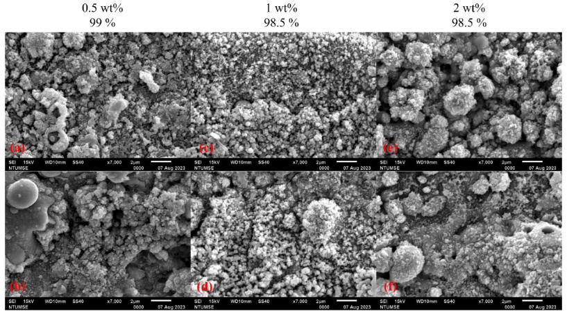
Silicon Nanoparticles Sintering
With the rise of an Intelligent Living System, wearable electronic devices are one of the key technologies. Therefore, how to apply semiconductor materials on flexible substrates has become a very important issue. Different from the traditional manufacturing of silicon thin film, which requires high temperature or high vacuum environment. This study uses a nanosecond pulse laser with a wavelength of 532 nm and a pulse duration of 8 ns to sinter p-type silicon nanoparticles. With its extremely short pulse dwell time, high energy density and the pattern control by galvanometer. We have successfully demonstrated laser sintering of a p-type Si nanoparticles (with dopant concentration of 5 × 10¹⁸ atom/cm³) on flexible substrates of PET in atmosphere environment.

Flexible Perovskite Solar Modules
As the demand for electricity rises and the gradual phasing out of fossil fuels becomes necessary, increasing the share of renewable energy has become a critical focus of research. In recent years, perovskite solar cells have seen their photoelectric conversion efficiency rise from 2.3% to 26.1%, approaching the efficiency of silicon-based solar cells that have been studied for a long time. As a third-generation solar material, perovskites have shown such rapid improvement in a short time, making it likely that they will soon surpass silicon-based solar cells. Furthermore, perovskite solar cells are thin-film materials that are lightweight, flexible, and easy to manufacture, making them ideal for development. However, for commercial use, large-area development is necessary.

Bi(2-x)Te3Sbx Films Deposition on
Flexible Substrates
With the vigorous development of wearable electronic devices, thermoelectric materials have a certain potential on wearable devices, which can replace batteries and allow devices to be used through electricity generated by temperature differences. Therefore, how to deposit the thermoelectric film on a flexible substrate and optimize its thermoelectric properties through a certain processing method has become the focus of this experiment. In this study, we deposit Bi₂ₓTe₃₋Sbₓ thermoelectric films on PET flexible substrates by sputtering deposition and annealing it in the atmosphere by continuous wave laser (λ = 532 nm) scanning system. We can find the best processing parameters by changing the laser power, scan speed and scan times. Finally, we successfully use laser annealing to reduce the resistivity by 60% and increase Seebeck coefficient. The power factor increase from 0.32 μW/cm * K² to 0.8 μW/cm * K². At last it is confirmed through bending test that the component can maintain the normal working range under 1000 bending at radius of 8 mm.
At the NEMO lab we investigate a vast range of research topics. These are some research ongoing and completed projects, as well as our technical capabilities and research expertise.
新能源及奈米材料實驗室旨在研究微奈米材料的雷射加工、柔性電子元件製造、太陽能電池製造等技術,方法是「結合理論、模擬與實驗」。目前的研究主題有:(1) 鈣鈦礦電池模組的全雷射製造技術;(2)奈米顆粒的雷射燒結成膜技術,譬如鋁摻雜的氧化鋅奈米顆粒、矽奈米顆粒等;(3)雷射退火對碲化鉍薄膜熱電性質的提升;(4) 奈米銀線的雷射焊接技術。